
How Korea’s Semiconductor Yield Optimization AI Impacts US Chip Costs
Let’s talk about something that sounds nerdy but hits your wallet in the most unexpected ways요
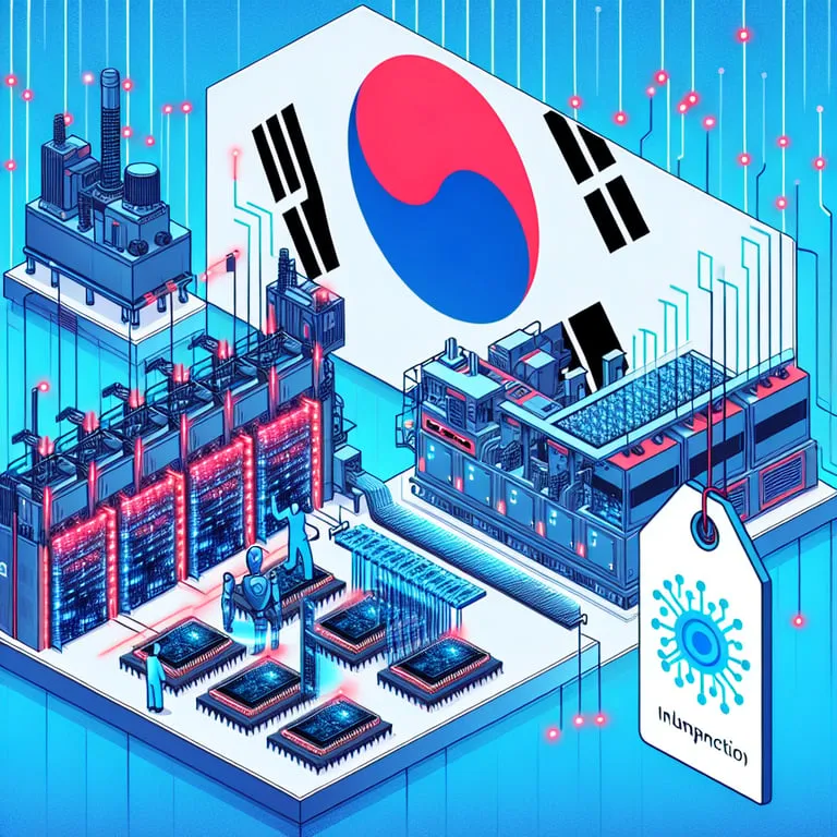
Korea’s fabs have been quietly turbocharging their yield with AI, and in 2025 that shift is bending the price curve for US chips in real time다
If you’ve wondered why HBM memory quotes feel a hair softer or why GPU build-of-materials look a touch less brutal than last summer, a lot of that traces back to smarter yield control upstream요
This is one of those stories where a few basis points of yield translate into hundreds of dollars saved per board, and that’s the kind of math I love walking through together다
Grab a coffee and let’s unpack it, friend요
The new reality of yield driven pricing
From defect density to dollars
Yield is the percentage of good die that survive fabrication and test, and the math is unforgiving다
For a given die area A and defect density D0, a common first-cut model is Y ≈ exp(−A·D0), which means tiny changes in D0 can swing output dramatically요
On advanced nodes and big dies, a 2–4 percentage point yield gain can cut cost per good die by 8–15% depending on wafer price and die size다
US buyers feel this as lower quotes, better availability, or tighter variance in delivery schedules because less scrap and rework ripple through the chain요
EUV stochastics and AI fixes
At EUV layers, randomness in photon shot noise and resist chemistry creates line-edge roughness and micro-bridging that cap yield다
Korean fabs feed petabytes of inspection images and tool logs into models that adjust dose, focus, and resist processes wafer by wafer요
AI-guided run-to-run control can trim critical dimension variability by 10–20% on sensitive layers, raising parametric yield without extra metrology passes다
It’s not magic, it’s statistics plus feedback, but when done at scale the savings compound fast요
HBM and AI accelerators price link
HBM stacks are assembled from known-good-die and through-silicon vias, so stack yield is multiplicative across layers다
A 2% per-die yield bump at the base die or DRAM chiplet level can push overall stack yield up by 3–6% depending on stack height and redundancy sparing요
In 2025, US accelerator makers whose BOMs are 30–45% HBM by cost see those points drop straight into margin or lower ASPs for hyperscalers다
If you’ve noticed procurement teams smiling a bit more when HBM3E quantities clear, this is why요
Foundry versus memory dynamics
Logic foundry economics hinge on mask counts and reticle-limited dies, while DRAM economics hinge on wafer throughput and stack integration다
Korean players sit at the intersection with both cutting-edge foundry and world-leading HBM lines, letting AI learn across different failure modes요
Insights from wafer sort and burn-in can now inform earlier litho or deposition tuning, closing loops that used to take weeks다
Shorter learning cycles mean US customers aren’t paying for long stretches of yield ramp like they did in past generations요
Inside Korea’s fab AI toolbox
Advanced process control and virtual metrology
APC adjusts recipes after each run based on sensor drift, while virtual metrology predicts film thickness or line width from tool signals without measuring every wafer다
Korean fabs report 30–60% fewer physical metrology steps on stable layers with VM, cutting cycle time and keeping WIP moving요
Fewer holds mean less queue time and less defect accumulation, which translates into higher effective throughput다
That shows up downrange as steadier allocation for US buyers when quarterly demand swings hit요
AI defect classification at scale
Automated optical inspection and e-beam tools spit out mountains of images, and deep models sort nuisance from killers with 95–99% precision depending on layer and topology다
Faster classification means root-cause analysis can happen during the same shift, not the next build cycle요
By pruning false alarms, fabs avoid overcorrecting and keep parametric yield from yo-yoing다
It sounds small, but even a 1% reduction in misclassification can save millions per quarter at high volume요
Digital twins and reinforcement learning
Full fab digital twins simulate queueing, tool matching, and maintenance schedules, letting RL agents optimize dispatch rules다
Cutting average cycle time by 5–10% reduces WIP exposure to contamination and drift, quietly nudging yield up요
Add predictive maintenance and you minimize unplanned downtime that forces recipe restarts and scrap다
US customers experience this as more predictable lead times and fewer last-minute reschedules요
Design technology co-optimization with AI
On the design side, AI helps select cell libraries, floorplans, and redundancy schemes that are friendlier to manufacturing다
Samsung and partners have showcased flows where ML recommends OPC and hotspot fixes before tape-in, not just post-route signoff요
When design-for-yield improves, wafer yield improves, and pricing conversations get less tense faster다
It’s a simple loop—better patterns, fewer stochastic failures, happier procurement teams요
Transmission channels to US costs
Component pass through into GPUs and servers
A GPU module’s cost stack includes silicon, HBM, substrate, assembly, test, and logistics다
If wafer yield improves 3%, cost per good die drops, and that saving often flows through negotiated cost-down clauses by 30–70% of the nominal gain요
For server builders, even a 1–2% module-level reduction can free budget for power delivery upgrades or faster networking다
This is why yield stories upstream show up as better TCO math in US data centers요
Equipment learning shared across borders
Korean fabs run fleets of US-made tools from KLA, Applied Materials, Lam Research, and ASML’s EUV stack다
When Korean teams co-develop AI recipes with these vendors, the know-how travels with software updates and field apps into US fabs too요
That convergence means a recipe fix in Hwaseong or Icheon can quietly benefit a line in Austin or Chandler within weeks다
The network effect compresses the time between insight and lower cost in the US market요
Contracting structures and price formulas
Many supply agreements tie pricing to wafer cost, yields, and scrap allowances with quarterly true-ups다
When measured yield beats the assumed baseline, credits or lower forward prices kick in after audits요
In 2025 more deals are embedding shared-savings clauses for AI-driven yield gains, aligning incentives elegantly다
The net effect is that US chip costs drift down faster once the models stabilize요
Lead times, cycle time, and carrying costs
Better yield reduces rework and shortens average cycle time, which lowers buffer inventory needs다
Lower inventory trims carrying costs by basis points that actually matter in big silicon programs요
Finance teams notice when days of inventory drop and cash conversion improves, even if the headline ASP barely moves다
That’s yield AI quietly paying dividends in places you don’t see on a die photo요
What the numbers say
Yield elasticity of cost per die
Consider a 300 mm wafer on an advanced node with an all-in cost of $16,000–$20,000 depending on mask count and EUV utilization요
If a large die yields 60% and moves to 64%, cost per good die falls roughly 6–10% after accounting for test and packaging escape rates다
On smaller dies going from 92% to 95% can still shave 3–5% off COGS because test and assembly scale with good output요
Multiply that by thousands of wafers per month and you see why CFOs obsess over a single yield point다
HBM cost stack and AI’s opex offset
HBM’s cost is wafer cost plus TSV, wafer bonding, thinning, test, and assembly with known-good-die selection요
AI that lifts sort accuracy and reduces retest can cut effective opex per stack by 3–5% and improve usable output by similar amounts다
For US accelerator vendors where HBM is a third to nearly half of BOM, that’s a serious lever요
Even when ASPs stay firm, availability improvements reduce spot buys and expedite fees다
Case sketch for an advanced logic die
Take a big compute die near reticle limit where you might only see tens of good die per wafer요
If AI-driven dose and focus optimization plus hotspot suppression nets a 3-point yield gain, you could free double-digit dollars per chip even after higher metrology spend다
Layer that with a 5% cut in cycle time via dispatch optimization and you compress working capital needs요
Stack enough of these tweaks and the module-level BOM eases by low single digits, which is huge at scale다
Sparing, redundancy, and binning
Redundancy at SRAM arrays, spare compute units, and smart binning all convert borderline die into usable SKUs요
AI improves the prediction of which die can be recovered and how to bin them without risking returns다
That shifts yield from hard-good to revenue-good, which is what ultimately drives US price curves요
The better the models, the fewer surprises at board bring-up and field return stages다
Risks, constraints, and policy
Data access and privacy in fabs
AI needs data, but fabs guard process windows and defect maps like crown jewels요
Federated learning and tightly scoped data rooms are becoming the compromise to let models learn without leaking secrets다
If data pipelines slow, model quality stalls and yield gains plateau요
US buyers should watch for signs of data friction because it foreshadows pricing stickiness다
Model drift and false positives
Process windows shift as tools age and chemistries tweak, and models can drift요
False positives trigger unnecessary recipe changes that hurt yield more than help다
The best teams run online monitoring with shadow deployments and A/B lanes to validate changes요
If you hear about excessive recipe churn, expect short-term volatility in quotes다
Export controls and alliances
Controls on AI hardware, EDA, and fab software shape who can share what and where요
Korea US alignment has generally improved knowledge flow, but edge cases still require careful licensing다
Any hiccup in tool software updates or cloud access can delay model deployment by quarters요
That shows up as slower cost-downs in US programs that were counting on those gains다
Talent and compute constraints
Training fab-scale models needs ML engineers who understand plasma, litho, and wet cleans plus serious compute요
Korean giants have built those hybrid teams, but everyone’s fishing in the same talent pool다
If compute budgets tighten or hiring lags, improvements might switch from step-changes to slow drips요
Plan for variability rather than assuming a straight-line glide path다
What US buyers can do now
Negotiate shared savings and telemetry
Push for contracts that share the benefit when measured yields beat the baseline요
Ask for anonymized process telemetry summaries that justify the adjustments, not just a new price card다
Transparency builds trust and accelerates cost-down cycles요
Vendors who believe in their AI will meet you halfway다
Qualify multi source HBM and substrates
Spread risk across at least two HBM sources when feasible and keep substrate vendors in a competitive posture요
Diversification cushions you if a yield model stumbles at one site다
When both sources are improving via similar AI, you benefit twice over요
This also tightens delivery windows when programs scale다
Align test strategies with factory AI
Tune your burn-in and system test to match fab-side binning so you don’t overtest or undertest요
Share field-return signatures back into fab models through structured feedback loops다
Closing that loop can convert marginal die into solid performers instead of rejects요
It’s a quiet way to reclaim margin without sacrificing reliability다
Build internal cost transparency
Maintain a living cost model that maps wafer price, yield assumptions, and assembly factors to module cost요
When a supplier claims a 3% yield gain, you’ll know exactly what that should mean to your price and lead time다
Data-driven conversations get you to yes faster and keep relationships healthy요
Your finance and engineering teams will thank you later다
The bottom line
In 2025, Korea’s yield-optimization AI is not just a cool lab story, it’s a line-item shift in US chip economics요
A few points of yield turn into real dollars when wafers cost five figures and dies push reticle limits다
As AI tightens process control, streamlines inspection, and smartens binning, the benefits cascade into HBM stacks, GPU modules, and eventually cloud TCO요
If you’re buying, building, or budgeting for silicon in the US, riding this wave thoughtfully can make your quarter feel a lot brighter다
That’s the quiet power of yield—small numbers, big impact, and a friendlier bottom line요
답글 남기기