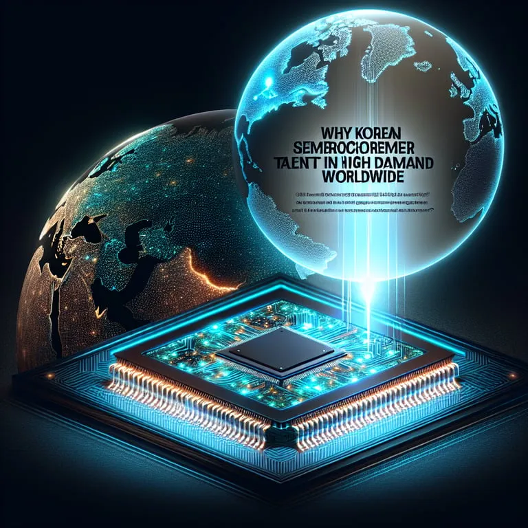
Why Korean Semiconductor Talent Is in High Demand Worldwide
It’s 2025, and every conversation about chips seems to circle back to Korea, doesn’t it요

From AI accelerators to the tiniest power management ICs, Korean engineers keep showing up where the hardest problems live다
You can feel it in hiring pipelines, in visa queues, and in conference hallways after keynotes요
There’s a reason the world is knocking on the same door, and it’s not just about famous brand names다
It’s about a culture of yield, a muscle memory for ramp, and a playbook for scaling that’s been battle tested across nodes and product cycles요
Let’s unpack that together, like old friends swapping notes after a long day on the fab floor다
- Korean semiconductor talent blends deep theory with shop floor instincts요
- Experience in HBM, advanced packaging, EUV, and GAA translates directly to 2025 roadmaps다
- Yield ramp discipline and cross functional problem solving are the real superpowers요
Deep Roots That Built a World Class Pipeline
Education that maps to fab realities
The talent story starts with schools that teach transistor physics the way athletes train muscle groups요
KAIST, POSTECH, SNU, and UNIST run labs where students debug line edge roughness on EUV resist or measure D0 on test vehicles before they ever visit a hiring fair다
Coursework weaves TCAD, SPICE corner analysis, and device reliability with hands on PVD, CVD, and CMP modules요
By graduation, many have already lived through a mock tapeout and a yield excursion postmortem complete with 8D reports다
Capstone projects mirror real fab bottlenecks, from photo dose window tuning to EMIR closure on dense SRAM macros요
National scale bets that didn’t blink
Korea doubled down on memory, materials, and equipment partnerships early, then kept iterating through crises다
When DRAM swung from boom to bust, teams learned cost discipline, statistical process control, and how to squeeze PPA under brutal ASP pressure요
Those cycles hardened engineers who can tune a photo recipe at 3 a.m. and still present a clean Pareto by 9다
That grit shows up now in AI memory, advanced packaging, and foundry ramps that can’t afford second tries요
Policy, academia, and industry formed tight loops that reduce the distance from research to rollout다
The big two and the ecosystem around them
Samsung Electronics and SK hynix are the headlines, but the ecosystem spans materials, gases, test, and design houses that form a full stack요
Suppliers like Soulbrain, Dongjin Semichem, SKC, and key tool partners built feedback loops where a chemistry tweak and a tool recipe change co evolve in days다
That proximity lets Korean engineers practice DTCO and even STCO with a speed many regions envy요
When your neighbor can bring a revised slurry or a new dielectric sample by lunch, learning cycles compress fast다
Startups plug into this network quickly, so new ideas meet pilot lines before they go stale요
Skills the World Needs Right Now
HBM know how that powers AI
AI training blew past bandwidth limits, and HBM3E became the new oxygen for accelerators다
Korean teams led 8 high and 12 high stacks, wafer thinning below 50 μm, and thermal budgets that keep 1 TB/s per stack stable under full load요
Engineers who can balance 9.2 Gbps per pin signaling with warpage control and power integrity across the interposer are rare and wildly valuable다
As HBM moves toward wider interfaces and hybrid bonding with sub 10 μm pitch, that scarcity only grows요
Field experience with TSV reliability, die to die test, and thermal path optimization makes resumes read like playbooks다
Advanced packaging and chiplets
Korea’s packaging playbooks stretch from 2.5D interposers to 3D stacking, branded as I Cube and X Cube on the foundry side요
Engineers here live and breathe micro bump reliability, underfill rheology, and interposer stitching beyond a single reticle다
They debug power delivery noise with EMIR signoff that actually matches silicon in the lab요
Chiplet era integration means partitioning RTL, floorplanning across dies, and co optimizing package and board, and that cross boundary literacy is a Korean forte다
Expect stronger co design flows that tie EDA constraints to substrate stackups and thermal budgets from day one요
EUV and GAA manufacturing
Being early on GAA taught process teams to choreograph gate cut, channel stress, and nanosheet uniformity across double digit EUV layers다
Litho groups battle stochastic defects with dose optimization, resist tuning, and clever SMO while etch tunes selectivity to avoid line collapse요
Device and integration engineers run DOE after DOE to lift SRAM Vmin without wrecking logic performance다
The same crew is already preparing for High NA EUV handoffs, from overlay budgets to pellicle thermal limits요
That mix of physics, metrology, and integration is exactly what 2 nm class nodes demand다
Yield ramp as a team sport
Yield is the passport stamp that travels well요
Korean fabs run SPC with ruthless clarity, marry KLA defect maps to e test signatures, and treat every excursion as a systems problem다
That habit produces leaders who can run a morning MRB, triage root causes, and push a fix into production by the next shift요
In a world where every month of delay costs hundreds of millions, that’s gold다
Playbooks for excursion response, guardbanding, and rapid reticle requal reduce risk on new lines요
Why Demand Spikes In 2025
The AI buildout refuses to slow
GPU, NPU, and accelerator roadmaps keep pulling in memory bandwidth and low latency packaging, and the world can’t hire HBM veterans fast enough다
You see it in job requisitions asking for TSV failure analysis, hybrid bonding pilot lines, and interposer RDL modeling with 2 2 2 design rules요
Korean resumes check those boxes because they’ve wrestled with the dragons in production, not just in slides다
That credibility shortens risk reviews and gets programs greenlit faster요
As inference scales at the edge, advanced packaging talent becomes just as strategic as core logic design다
New fabs need experienced hands
The CHIPS era brought new lines online in the United States, Japan, and Europe, and every new toolset needs owners who have lived through a ramp요
Samsung’s expansion in Texas and SK hynix’s advanced packaging footprint in the Midwest create gravity wells for talent that pull from Seoul to Austin and beyond다
Tool vendors from deposition to metrology are also fishing in the same pond, because customers want application engineers who speak fab, not just spec sheets요
Koreans who can teach a chamber its manners while tuning process windows on the fly are exactly what these sites need다
Design and system co optimization goes mainstream
As chiplets and advanced packaging spread, the wall between design and manufacturing keeps crumbling요
Teams now run DTCO loops that swap cell libraries, change bump maps, and retime fabrics to fit thermal and mechanical limits다
Engineers comfortable in this soup of tradeoffs save quarters of calendar time, and Korea has trained a lot of them through memory and logic co development요
In 2025, that blended skill set is the difference between a paper launch and a product that ships in volume다
Scarcity plus urgency equals premium
Everyone is courting the same profiles, so offers have leveled up with relocation support, research time budgets, and fast tracks to technical fellow roles요
Companies that combine tough problems with a humane culture win, and candidates are savvy about asking for both다
The days of unlimited crunch are gone, and Korean engineers are choosing employers who can scale without burning out their best people요
That shift is healthy for the industry and, honestly, overdue다
What Sets Korean Engineers Apart Beyond the Resume
Speed that doesn’t skip the science
There’s a famous phrase about doing everything fast, but the secret is methodical speed anchored in data요
You’ll see engineers run fractional factorial DOE, apply Bayesian updates to narrow suspects, and land on fixes that stick다
Quick isn’t sloppy here, it’s a disciplined loop of measure, learn, and deploy요
That rhythm compounds over quarters until ramp curves look almost unfair다
Communication across silos
Korean teams rotate people through device, process, test, and packaging more than most, and it shows in how issues get framed요
Instead of tossing problems over walls, they pull the right folks onto the same whiteboard, from RF designers to substrate vendors다
The result is fewer blind spots and fewer late surprises, which is priceless when tapeout windows are non negotiable요
It also makes cross border projects less brittle because context travels with the people다
Craftsmanship with tools and materials
There’s real pride in understanding how a tool breathes through a day, not just which buttons to push요
Engineers notice when a pump tone shifts, when a chamber’s seasoning drifts, and when a slurry lot behaves a hair off spec다
That craftsman mindset keeps small deviations from snowballing into yield killers요
It’s subtle, but you feel it the moment you walk a line with a seasoned Korean crew다
Global mindset anchored at home
Many Korean engineers spend time at imec, in US research centers, or inside customer sites, and they come back fluent in multiple playbooks요
That makes them natural bridges on multinational teams, equally comfortable arguing a corner case with EDA vendors or negotiating a spec with an OSAT다
The local ecosystem benefits too, because those lessons get folded back into university labs and supplier roadmaps요
It’s a flywheel powered by people, not just capital다
Practical Advice For Teams Hiring Korean Semiconductor Talent
Meet them where they are
Partner with universities and labs that already run tapeout like a sport, and sponsor capstone projects that map to your roadmap요
Candidates light up when they see their thesis topic mirrored in your product plan다
Host technical talks that go beyond marketing slides and invite engineers to challenge your assumptions요
Respect is a two way street, and good questions are the fastest way to show it다
Design interviews that reflect real work
Skip trivia and focus on debugging narratives, yield excursions, and cross functional tradeoffs요
Ask how they would bring HBM3E into a new package with a different thermal stack, or how they would validate a High NA overlay budget다
Listen for the structure of their thinking, the metrics they grab first, and how they decide when to stop analyzing and start fixing요
That’s where the magic lives다
Offer growth that compounds
Spell out paths into technical leadership, rotations across packaging and design, and time carved out for patents and papers요
Many candidates want to keep a hand on tools while mentoring younger engineers, and they thrive when you make that explicit다
Pair them with peers who care about the craft, not just the quarterly slide deck요
People stay when they can see their future from here다
Support life outside the fab
Global moves are exciting and stressful, so help with family relocation, language learning, and community building요
A great daycare, a realistic on call schedule, and a manager who respects downtime go further than another signing bonus다
Well supported teams ship better chips, because they can sprint when it counts and recover when they need to요
It’s that simple and that hard다
Looking Ahead Together
The road beyond HBM
Memory isn’t standing still, and research on stacked architectures, new dielectrics, and smarter power delivery is accelerating요
Korean labs are poking at the edges of what TSVs and hybrid bonding can do while eyeing reliability over tens of thousands of hours다
Expect ideas like backside power and algorithm aware memory scheduling to leak from papers into products faster than you think요
Teams who can straddle device physics and system performance will set the pace다
High NA and the yield frontier
As High NA EUV enters production, overlay budgets tighten, line edge roughness takes center stage, and metrology must get smarter요
The talent fluent in shot noise, stochastic modeling, and resist chemistry will shape what’s possible at 2 nm class nodes다
Korea’s mix of device, litho, and integration expertise is well suited to that frontier요
And the world will keep calling when the ramps get real다
Beyond silicon alone
Materials innovation from packaging substrates to thermal interface materials will matter as much as transistors요
Expect cross disciplinary teams that blend polymer science, mechanical engineering, and RF design to become the norm다
Korean engineers who already work across those borders will feel right at home요
That versatility is why their calendars fill up so quickly다
A friendly note before we log off
If you’re building chips in 2025, you’re in the arena, and it’s okay to admit it’s a little wild right now요
Reach out, compare notes, and don’t be shy about recruiting from the places that have done the hard things under bright lights다
Korean semiconductor talent didn’t appear by accident, it grew through years of grit, generosity, and shared wins요
Bring that energy onto your team, and you’ll feel the difference in your ramp curves and in your culture다
And if you’re one of those engineers reading this, thank you for the craft, the patience, and the midnight fixes that no one outside the lab will ever see요
We’re all better for it, and the next chapter looks pretty exciting together다
답글 남기기